


PowiGaN Technology
PowiGaN is Power Integrations’ internally developed gallium nitride (GaN) technology. PowiGaN switches replace the traditional MOSFETs on the primary side of PI’s highly integrated offline flyback switcher ICs, reducing switching losses and enabling chargers, adapters and open frame power supplies that are more efficient, smaller and lighter than silicon alternatives. Power Integrations continues to lead the advancement of GaN technology, expanding the switching voltage and elevating GaN as a mature, dependable semiconductor technology for even the most demanding applications.
Pioneering High-Voltage GaN Power Devices for a Wide Range of Applications

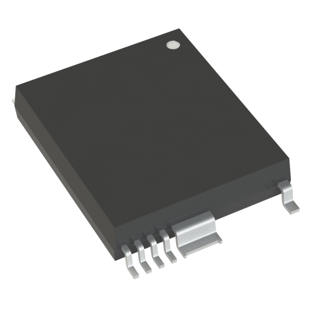
InnoSwitch3-EP for Appliances and Industrial Use
- 750 V, 900 V or 1250 V PowiGaN switch
- Power Integrations most versatile single-switch flyback power supply IC family offers three voltage ratings with GaN switches, in addition to silicon and SiC options. Design engineers can choose the switching option most suitable to their applications without altering the design.


Highest Level of Integration in USB PD and Fast-Charging
InnoSwitch5-Pro
900 V PowiGaN, ZVS without active clamping, supporting 28 V USB PD Extended Power Range
InnoSwitch4-Pro
750 V PowiGaN, ZVS with ClampZero, digitally controllable via I²C interface
InnoSwitch4-CZ
750 V PowiGaN, ZVS with ClampZero for maximum efficiency
InnoSwitch3-PD
750 V PowiGaN, built-in USB-C and USB PD controller
InnoSwitch3-Pro
750 V PowiGaN, digitally controllable via I²C Interface
InnoSwitch3-CP
750 V PowiGaN for constant power charging
LYTSwitch-6
750 V PowiGaN for LED lighting and ballast
MinE-CAP
for reducing capacitor size in chargers, paired with InnoSwitch ICs
Resources
Related Content
- PowiGaN-Based Primary-Side Power Switches Extend the Power Range of InnoSwitch3 IC Families
- PowiGaN Technology
Related Videos

